Background
In polarized target experiments, it is important to be able to measure the polarization of nuclear targets. The Q-meter is a method of doing this. The nuclear target is placed in the inductive part of an LC circuit, and the circuit is tuned to have the same resonant frequency as the nuclear target. The frequency of the RF voltage is modulated, from which one can detect changes in the circuit's Quality Factor (the "Q" in "Q-meter"). From this quantity, one can obtain a measurement of the polarization of the target. For more detail on the method, see the Liverpool Q-Meter Guide.
The particular design for this Q-meter comes from the University of Liverpool. There are five printed circuit boards (referred to as PCB 1, PCB 2, ..., etc.) which constitute the Q-meter circuit. The University of Virginia's PT Group has several of these Q-meters which were built some time ago. Some of them are fully functional, while others are not - for instance, some do not produce a curve, while some produce an inverted curve. The PT Group also has access to the Q-Meter Guide (previously mentioned), as well as the Q-meter's design documents, which detail the designs of the metal frames and the PCB's.
Because of the convenience of this device, and the access to the design documents, it could be a productive effort to try to fix the non-functional Q-meters, and to construct new Q-meters. The way to go about this is to make new PCBs, preferably with off-the-shelf components or modern replacements for obsolete components.
Method
The first step was to design the PCBs in a modern CAD software. Following the Q-meter's design documents, each of the five PCB's was reconstructed in KiCAD, a free and open-source CAD software for designing printed circuit boards.
Designing a circuit board in KiCAD follows several steps which will be briefly explained:
1. Schematics
 |
|
|---|---|
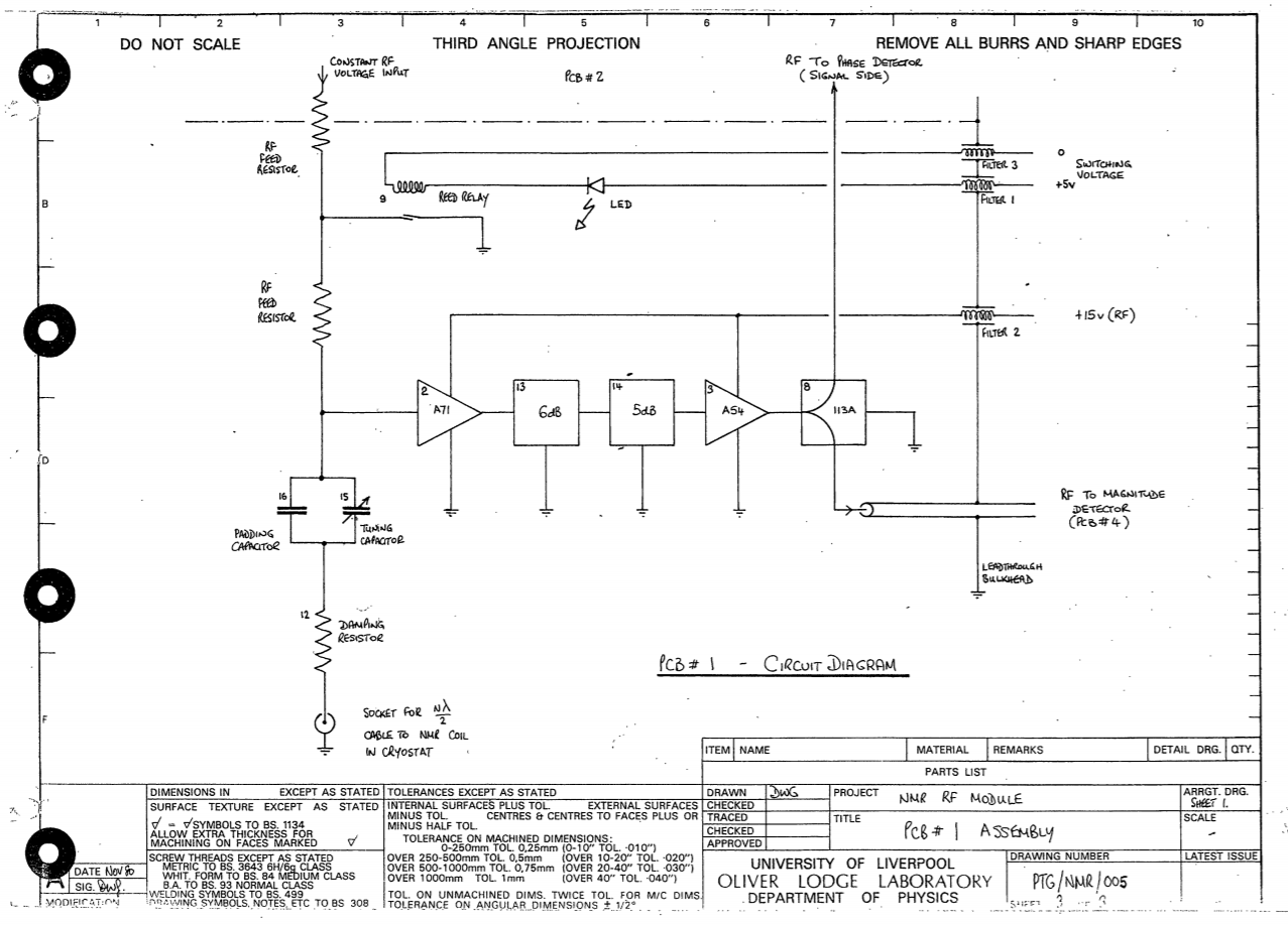
| The original schematic for PCB 1 in the design document | The recreated schematic for PCB 1 in KiCAD |
First, one must construct the schematic for the circuit. Fortunately the design documents contained schematics for each PCB. Often, the user will need to construct a custom Symbol for one of the circuit's components, because the KiCAD library mostly contains common Symbols (resistors, capacitors, etc.) and likely will not have one tailored to the exact component. For instance, the 113A Symbol in the above schematic (rightmost square) had to be drawn from scratch, taking into account the number of pins and labels for each. KiCAD has a built in tool for drawing new components.
2. Laying out the PCB
The next step is to actually lay out how the circuit will look. The difference between this and designing the schematic is that, while the schematic tells KiCAD what components should be connected to which other components, the PCB editor actually determines how the board will be physically laid out.
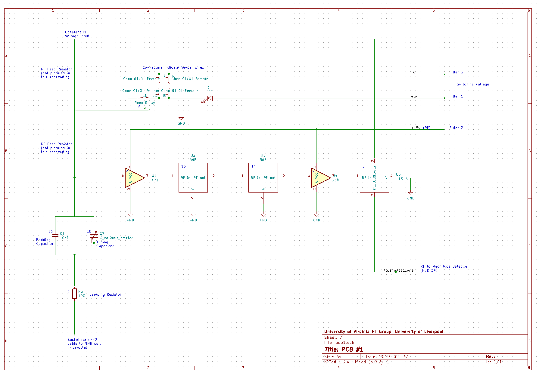
To illustrate, the following image is what the PCB looks like when one first loads their schematic into the PCB editor:
|
|---|
| PCB 1. The footprints are initially disorganized in the PCB editor. |
There are white lines which denote connections between components - this information is received from the schematic (specifically the Netlist file, which is generated from the Schemati). The user must move these components around, and draw traces to complete a connection between components.
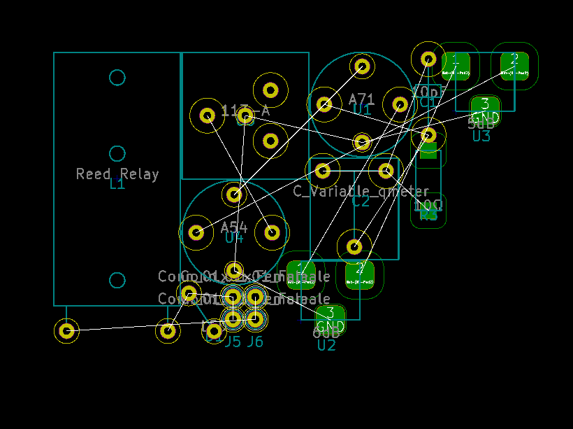
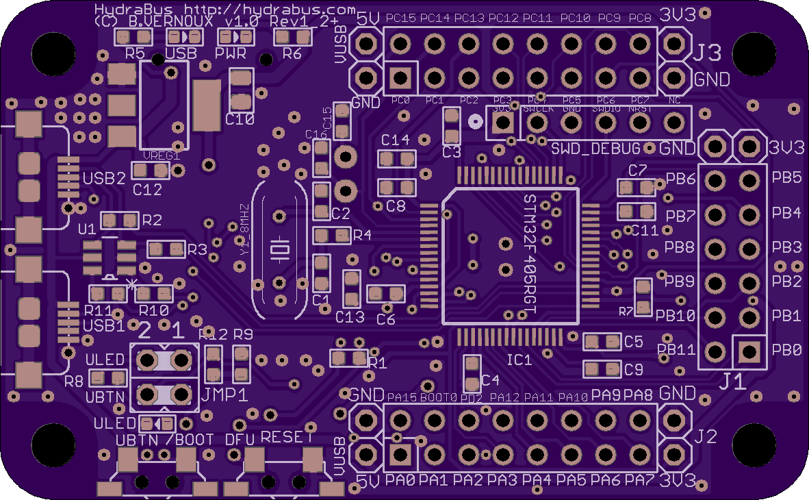
The completed PCB design is shown below, with the ground planes made transparent so that the traces (the thick green lines) are more clearly visible.
|
|---|
| Finished PCB 1. |
As with the schematic editor, there are representations of the circuit components. They are called "Footprints" here, and they are different from Symbols in that they must represent how the component will physically exist on the board. The Footprint will tell the KiCAD software (and, therefore, the manufacturer of the PCB) where the holes for the pins must be drilled and where to place copper for its connections. KiCAD has an editor to create custom Footprints.
The layout of each PCB was designed to match the original PCBs as closely as possible. Some things to keep in mind were the boards' dimensions, the positions of traces which connect to other PCB's (such as the two traces in the middle of the right edge, of the PCB pictured above), the thicknesses of the traces, the clearance of the traces (space between the trace and the ground plane), and the area of the ground plane.
3. Manufacturing
|
|---|
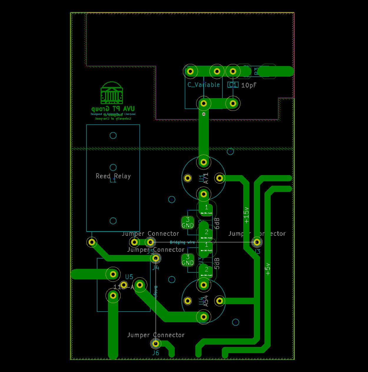
| PCB 1, uploaded to OSHpark. |
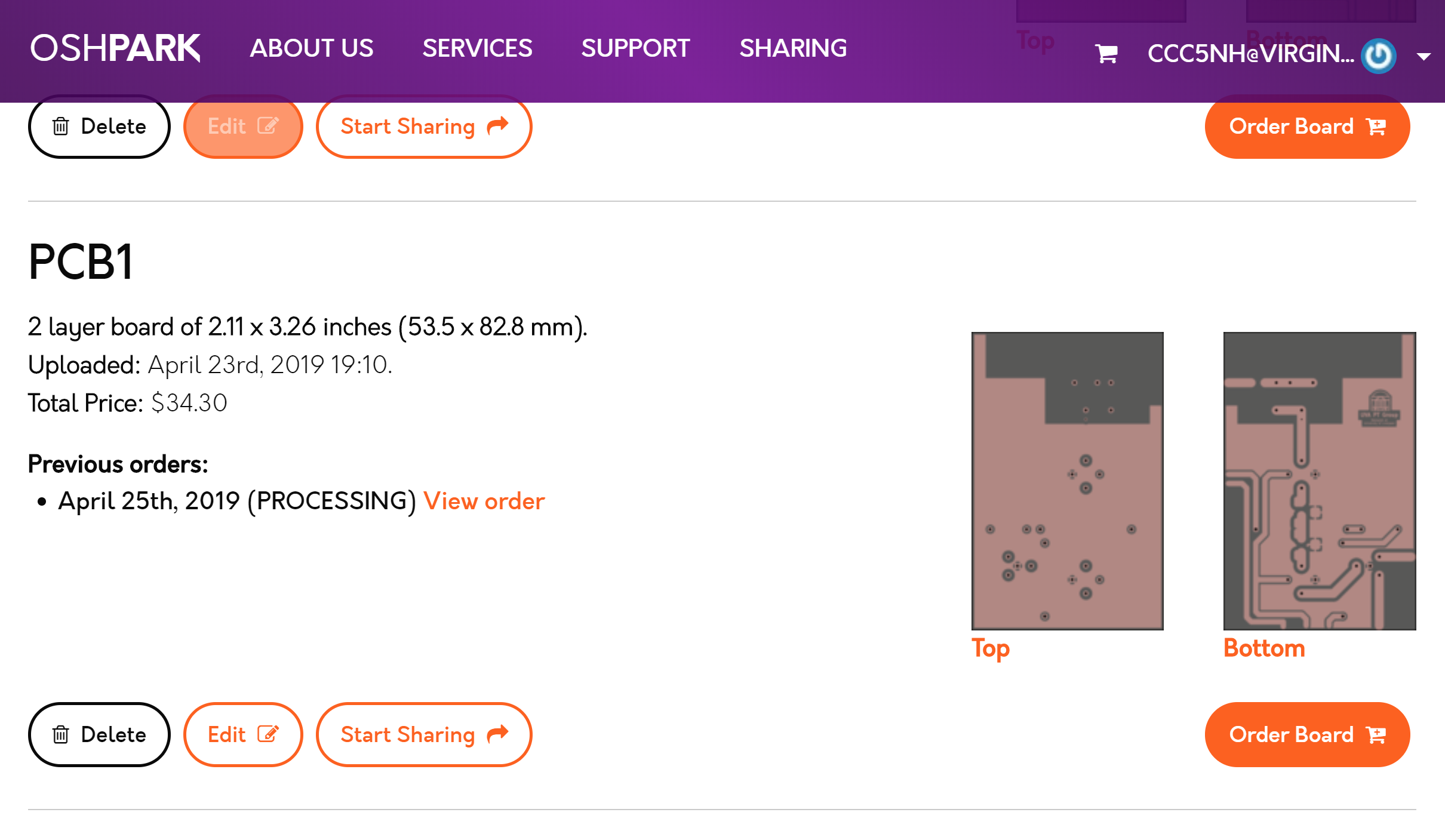
Once the PCB layout is complete, one must create "Gerber files" which are the industry standard format for designs of PCBs to be manufactured. KiCAD has the ability to create these from the PCB Layout editor, as well as to create "Drill files" which tell the manufacturer where holes should be drilled on the PCB.
The service used was called OSHpark. They have the advantage of decent prices, the ability to order a small number of PCBs at a time, and a simple and straightforward web interface. One simply must upload the Gerber files, and then place the order.
There are a few important things to note:
- PCB designs consist of "layers." For example, on a two-sided PCB, there will be a "Front Copper" layer and "Back Copper" layer, which have the traces meant for the front and back of the PCB, respectively. There is also the "Edge Cuts" layer which tells the manufacturer the perimeter of the board to cut around. There are "Silkscreen" layers which have useful symbols/text to be printed onto the board. There are also "soldermask" layers, explained below.
- A PCB typically has something called a "Soldermask" which is a layer of polymer that shields the copper traces underneath from oxidation. The Liverpool Q-meter design does not call for any soldermask, opting instead for gold plating. To match the original design, we ordered our PCBs with no soldermask layer. In CAD software, soldermask layers are typically "negative," meaning that rather than placing soldermask wherever the design is filled in, it actually places soldermask wherever the design is not filled in and keeps it away from filled zones. To order a PCB from OSHpark with no soldermask, one must go into KiCAD and place a filled zone over the entire board on both front and back soldermask layers.
- OSHpark offers gold-plated nickel over copper as a further way to protect the copper from oxidation. Even without soldermask, it is our expectation that this layer will protect the copper on our PCBs from oxidation.
|
|---|
| A sample design from OSHpark's website. The purple regions is soldermask (the darker lines are the copper traces underneath). The white text and white shapes are silkscreen. The pink areas are exposed copper. |
List of Parts
| Item | Description | Quantity per board | Modern replacement (if applicable) |
| RF Amplifier | A71 | 1 | |
| RF Amplifier | A54 | 1 | |
| RF Amplifier | GPD-402 | 1 | |
| RF Amplifier | GPD-403 | 3 | |
| RF Splitter | 113A | 1 | |
| Double Balanced Mixer | SRA-1 | 1 | |
| Detector Diode | BD3, back diode | 2 | |
| Chip Resistor | CR15, type B, 5%, 27Ω | 2 | |
| Chip Resistor | CR15, type B, 5%, 50Ω | 1 | |
| Chip Resistor | CR15, type B, 5%, 10Ω | 1 | |
| Chip attenuator | AC0103, 3dB, 50Ω | 3 | |
| Chip attenuator | AC0105, 5dB, 50Ω | 2 | |
| Chip attenuator | AC0106, 6dB, 50Ω | 2 | |
| Tuning capacitor | AP14E1, with insulated shaft | 1 | |
| Capacitor | 10 pF S. Mica | 1 | |
| Capacitor | 220 pF ceramic | 4 | |
| Capacitor | 1000 pF ceramic | 8 | |
| Capacitor | 0.1 µF ceramic | 2 | |
| Resistor | 150Ω thick film | 1 | |
| Resistor | 220Ω thick film | 1 | |
| Resistor | 330Ω thick film | 2 | |
| Resistor | 2.2kΩ thick film | 12 | |
| Resistor | 4.7kΩ thick film | 6 | |
| Trimpot | 10kΩ, 3262W-1-103 | 2 | |
| Dual Op Amp | OP-10 EY / LT1002 | 2 | |
| Op Amp | LF356N | 2 | |
| RF Inductor | 10 µH | 2 | |
| Lead Through Filter | 1251-001, EMI suppression | 14 | |
| SMA Jack | R.125-403, 4 hole flange socket | 3 | |
| SMA Plug | R.125-052, straight solder plug | 4 | |
| Multiway connector | DB-25P | 1 | |
| Multiway connector | DB-25S | 1 | |
| SMA Jack | 2004-7985, straight b'head jack | 1 | |
| Cable | BA50085, semi-rigid | 150 cms | |
| LED | 10 mA @ 2V, to fit 4mm hole | 1 | |
| Capacitor Drive | Type H | 1 | |
| Capacitor Drive knob | 412, multi-turn, lockable | 1 | |
| Capacitor Drive sleeve | Rubber coupling | 2 cms | |
| Solder tag | H3 | 1 | |
| Screw | M2.5 * 6mm, cheese head | 65 | |
| Screw | M2.5 * 16mm, c/sunk head | 7 | |
| Screw | M3 * 6mm, cheese head | 3 | |
| Interconnecting wire | 7/0.2mm, insulated copper | ||
| Interconnecting wire | 1/0.6mm, bare copper | 15 cms | |
| Sleeving | As required, for above | ||
| Solder | |||
| Reed switch | Mini-25, 7-12 AT | ||
| SMA Phase adjuster | 901-508, In-line adaptor | 1 | |
| Module frame assembly | PTG/NMR/002 | ||
| Capacitor drive assembly | PTG/NMR/003 | ||
| Reed relay assembly | PTG/NMR/004 | ||
| Lead through b'head assy. | PTG/NMR/011 | ||
| Star washer | 9.5mm 1/D, 17mm 0/D (max) | ||
| Washer | M2.5, plain, brass | ||
| Screw | M4 * 6mm, c/sunk head |
Files
Liverpool Q-meter Guide: LiverpoolQMeterGuide.pdf
Q-meter design document: qmeter_blueprint.pdf
KiCAD files (Most recent update: 4/23/2019): qmeter Boards.zip (Note: pcb3_fabrication and pcb4_fabrication contain the PCB layouts which were ordered. pcb3 and pcb4 contain schematics which more closely resemble the design document, but which are less convenient to construct in KiCAD because of how the dual op-amps are separated).
Just the Gerber files (Most recent update: 4/23/2019): Gerber_Files_for_PCBs.zip